
STUDENT REVIEW'S
At Igeeks Technologies, student satisfaction is our highest priority. Over the past 15years, we’ve proudly trained and mentored thousands of students across India through our internship programs, academic projects, and research guidance. Here’s what our students have to say about their experience:
-

Narsimha Reddy
Best Institute for Engineering students. I got wide range of project options here. Staff were very friendly and helpful. All the necessary documents were given on time. The teaching staff are all qualified and have the capability to design projects equivalent to industry standards. Had a great time here. Thanks to Igeeks Team.
-

Smitha Nair
I was an intern in Igeeks for a duration 1 year. Interns got lot many things to learn, execute, and responsibility. Managers are friendly,encouraging and supportive. Good environment with team members . Alot of opportunities to learn and grow.Thank you for routing my career.
-
Avi Avinash
Igeeks is the good institute for engineering projects. I learnt many things here. It is best place to learn about the Embedded systems.It was a good experience,very supportive and friendly faculty.
-
Sravanthi msrit
It is the best place for Machine Learning Projects, Projects will be completed as per the date no need to worry, it's a good choice for students. They help you to learn and do the stuff on your own. They will provide virtual help to students any part of the day. Very professional. Nice experience......
-
Anil Sharma
Writing thesis was never easy for me. While searching for someresources for thesis help, i got in touch with Igeeks. The work done by their team was appreciable. There were no grammatical errors and they also maintained proper format. I am totally satisfied with the quality work delivered.
-
Chaitanya Karumudi
Best Institute for IOT Projects. I got wide range of project options here. Staff were very friendly and helpful. All the necessary documents were given on time. The teaching staff here are all well qualified and have the capability to design projects equivalent to industry standards. Had a great time here. and its budget friendly.
-
Priscilla samuel
I have done my M.Tech project here recently on SBT Movie recommendation..i got good support and knowledge as well. So i recommend you, if you are seeking for the best project.
-
Samit kumar
We highly suggest Igeeks! I had four assignments due all within one week. Due to my work schedule and other commitments, I didn't have the time to finish all the assignments. I was anxious about using the services to write or edit my essays; however, I went to their office to find a friendly group of people who understood my demands and helped ease my anxieties. The customer service team was excellent and helped me receive my needed marks. I would not have been able to do it without them. Thanks for your support, team!
-
Paviksha
Thank you for the support in this project and we can get good support to the supporter for giving quick responce. Error or bugs correction skill also good. They have been supported from the beginning and the end of the project Supporter will also give good support to me. Thank you for your support...
-
Mahesh
It's a very good experience with Igeeks . Igeeks is a place where you can get plenty of projects on different domains. We can get a project with reasonable rate and under guidance of professionals. It's a good platform for projects they are very comfortable to communicate.....
-
Nageswara Rao
I have done my MBA project in this institution and the quality of project is good and they have guided nicely.
-
Vijayalakshmi
I have contacted Igeeks with a big challenge on a very tight deadline.. They came back with a flying colours in solving the issue within a time I expected.. Very polite and professional I strongly recommend this team..
-
Karthik
I am very great full to Dr. Waseem C sir for guiding me and giving me a complete clarity on my Finance MBA Desrrtation topic . It was not an easy topic given by my college but then Dr.waseem sir has helped me in the entire of my project . Thank you so much sir . Thank you for doing and giving my MBA desertation project sir.
-
Suraj
The project quality was very good, I like the way they provide all system development videos along with the kit. I had ordered the Vechical Tracking Project kit & am happy to have ordered from here.. no issues at all
-
Vignesh
They helped me a lot in my research work. They work on latest technologies and algorithms. I would say they are the best resource for any PhD perusing candidate. From defining problem statement till thesis submission they supported me. Thanks for Igeeks Team.
-
Rachana
I enlisted help to complete my assignment. They were extremely efficient and thorough in their work. I would get confirmation on every aspect. Everything is clear and transparent. They will, in the end, deliver on their word. The PhD team was very helpful and helped me to clear my doubts. One stop for all academic work...Would recommend.
-
Jinal
I engaged their service for help with Scopus research paper publications. My domain of research relates to Networking domain and the work was done with care and I was able to get acceptance for publication in a journal with impact factor of 3.5.
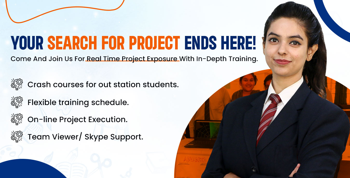
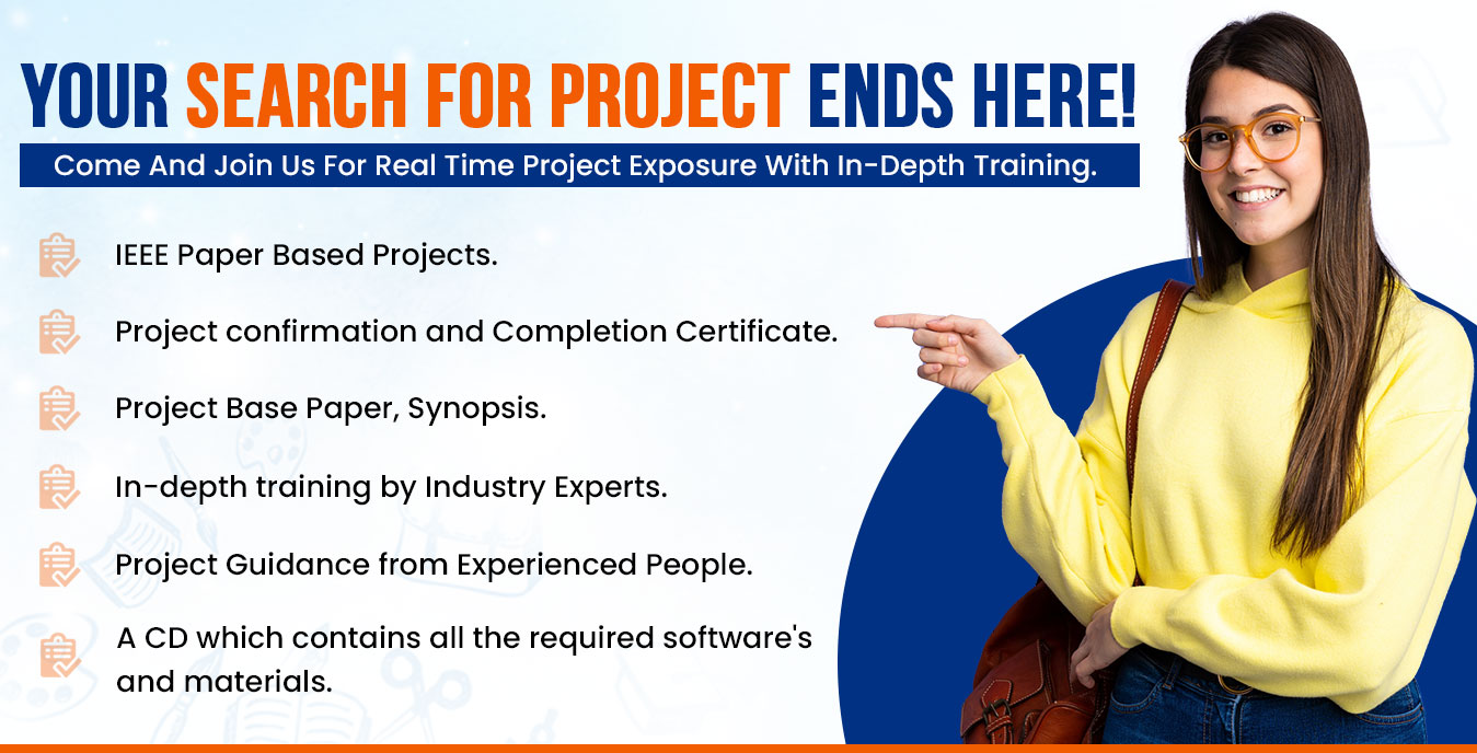
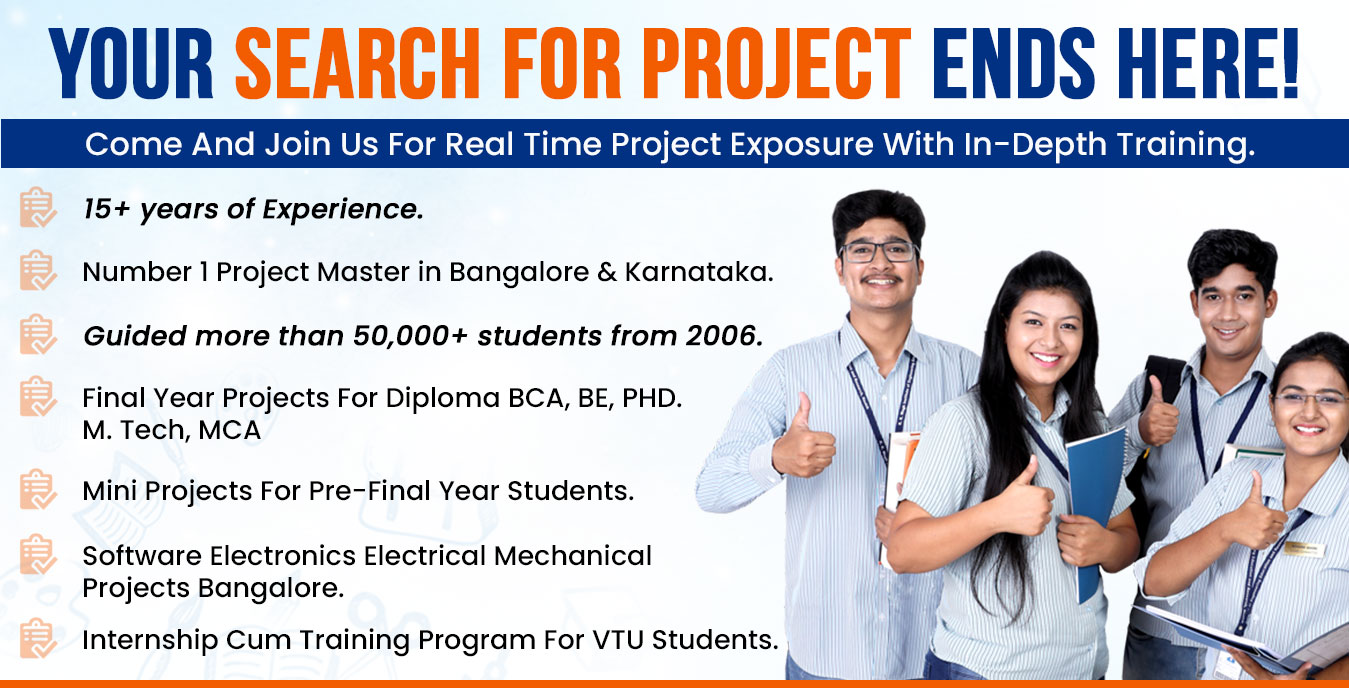
PROJECTS 2025-2026 
Ask For Your Projects
Igeeks is India’s largest edu-tech company with 15 years of experience and the creator of a unique and innovative live project making platform for students, which enable them to fill their education gap as well as to gain practical knowledge with real-time experience. Igeeks majorly focuses on Academic Project Development, Student internship, and Placement guidance.
"India's leading Academic Projects, Internships,MBA Projects & PHD Projects. 100% output guaranteed and fully customized projects are Implemeted.Igeeks is a Multi-Disciplinary Platform for BCA, Diploma,MCA, B.Tech, M.Tech, PhD Projects.We are known to deliver Quality assured projects, Plagiarism free documents, Journal Paper writing."
Our Award Winning Tech Team have trained thousands of students and have guided over 8000+ working projects via Practical Research based Project training, out of which some of the projects have won best project awards at various national & international competitions.More than 50,000+ satisfied customers got assistance from universities and affiliated colleges.
IGEEKS BEST'S 
Projects Offer For
- B.E (Computer Science)
- B. E (Electronics and Communication)
- B. E (Electrical and Electronics Eng.)
- B. E (Information Technology)
- B. E (Instrumentation Control and Eng.)
- M. E (Computer Science)
- M. E (POWER ELECTRONICS)
- M. E (CONTROL SYSTEM)
- M. E (SOFTWARE ENG)
- M. E (APPLIED ELECTRONICS)
- M. SC (IT , IT&M , CS&M, CS)
- MCA
- BCA
- B.Sc. (IT , CS)
- MD, MS, DNB, PhD
- MBBS
- Nursing
- PhD
- MBA
- BBA
Projects By Degree
- Engineering Final Year Projects.
- MTech Final Year Projects.
- Diploma Final Year Projects.
- BCA Final Year Projects.
- MCA Final Year Projects.
- MBA/BBA Final Year Projects.
- PHD Projects.
- Research Paper Writing.
- Journal Paper Writing.
- Capstone Projects.
- Assignment Services.
- PhD Thesis Writers
- Research Paper
- Publishers in Scopus
- International Assignment Writing
- MD Thesis Writing Services
- Internship for Engineering Students
- M.Tech Civil Engineering Projects
- MTech Power Systems Projects
- MTech VLSI Projects
- M.Tech EEE Power Electronics
- Best AI Final Year Projects
- Medical Thesis Writing Services
- Thesis writing for Medical
- Medical Research Paper Writing
- Nursing Dissertation Help
Technology We Cover
- EMBEDDED
- MATLAB
- VLSI
- ELECTRICAL
- PYTHON
- ANDROID
- NS2/NS3
- JAVA
- Arduino UNO
- Raspberry Pi
- GSM & GPS
- RFID
- Ansys
- Renesas
- SPSS
- IOT
- WSN
- NodeMCU
- Robotics
- Xilinx
- OpenCV
- PHP
Project Domains
- Artificial Intelligence
- Machine Learning
- Deep Learning
- Image Processing
- Data Science
- Cloud Computing
- Data Mining
- BlockChain
- CyberSecurity
- Signal Processing
- 5G networks
- MANET
- VANET
- Networking
- Mobile Computing
- Antenna
- Low Power VLSI
- Transistor Logic
- Core Memories
- Power Systems
- Power Electronics
- Electrical Drives
- Control Systems
- MBA MARKETING
- MBA FINANCE
- MBA HR
- MBA BUSINESS ANALYTICS
- MBA IT MANAGEMENT
- MBA PROJECT MANAGEMENT
- MBA OPERATIONS


0
YEARS OF EXPERIENCE
0
SOFTWARE PROJECTS
0
ELECTRONICS PROJECTS
0
MBA PROJECTS